- 非IC关键词
企业档案
- 相关证件:

- 会员类型:普通会员
- 地址:高新区舜泰广场8号楼8楼
- E-mail:376313735@qq.com
产品分类
产品信息
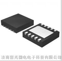
供应高压放大器 OP400GPZ 低失调、低功耗四通道运算放大器
替代器件AD8624 : Lower power and smaller package options
OP4177 : 精密、低噪声、低输入偏置电流、四通道运算放大器
GENERAL DESCRIPTION
The OP400 is the first monolithic quad operational amplifier
that features OP77-type performance. Precision performance is
not sacrificed with the OP400 to obtain the space and cost
savings offered by quad amplifiers.
The OP400 features an extremely low input offset voltage of less
than 150 μV with a drift of less than 1.2 μV/°C, guaranteed over
the full military temperature range. Open-loop gain of the
OP400 is more than 5 million into a 10 kΩ load, input bias
current is less than 3 nA, CMR is more than 120 dB, and PSRR
is less than 1.8 μV/V. On-chip Zener zap trimming is used to
achieve the low input offset voltage of the OP400 and eliminates
the need for offset nulling. The OP400 conforms to the industrystandard
quad pinout, which does not have null terminals.
The OP400 features low power consumption, drawing less than
725 μA per amplifier. The total current drawn by this quad
amplifier is less than that of a single OP07, yet the OP400 offers
significant improvements over this industry-standard op amp.
Voltage noise density of the OP400 is a low 11 nV/√Hz at
10 Hz, half that of most competitive devices.
The OP400 is an ideal choice for applications requiring multiple
precision operational amplifiers and where low power
consumption is critical.
SPECIFICATIONS
ELECTRICAL CHARACTERISTICS
@ VS = ±15 V, TA = +25°C, unless otherwise noted.
Table 1.
OP400A/E OP400F OP400G/H
Parameter Symbol Conditions Min Typ Max Min Typ Max Min Typ Max Unit
INPUT CHARACTERISTICS
Input Offset Voltage VOS0 μV
Long-Term Input
Voltage Stability
0.1 0.1 0.1 μV/mo
Input Offset Current IOS VCM = 0 V 0.1 1.0 0.1 2.0 0.1 3.5 nA
Input Bias Current IB VCM = 0 V 0.75 3.0 0.75 6.0 0.75 7.0 nA
Input Noise Voltage en p-p 0.1 Hz to 10 Hz 0.5 0.5 0.5 μV p-p
Input Resistance
Differential Mode
RIN MΩ
Input Resistance
Common Mode
RINCM00 GΩ
Large Signal Voltage
Gain
AVO VO = ±10 V
RL = 10 kΩ 5000 12, V/mV
RL = 2 kΩ V/mV
Input Voltage Range 1 IVR ±12 ±13 ±12 ±13 ±12 ±13 V
Common-Mode
Rejection
CMR VCM = 12 V35 dB
Input Capacitance CIN 3.2 3.2 3.2 pF
OUTPUT
CHARACTERISTICS
Output Voltage Swing VO RL = 10 kΩ ±12 ±12.6 ±12 ±12.6 ±12 ±12.6 V
POWER SUPPLY
Power Supply Rejection
Ratio
PSRR VS = 3V to 18V 0.1 1.8 0.1 3.2 0.2 5.6 μV/V
Supply Current per
Amplifier
ISY No load25 μA
DYNAMIC PERFORMANCE
Slew Rate SR 0.1 0.15 0.1 0.15 0.1 0.15 V/μs
Gain Bandwidth
Product
GBWP AV = 500 kHz
Channel Separation CS VO = 20 V p-p,35 dB
fO = 10 Hz 2
Capacitive Load
Stability
AV = 1,
no oscillations
nF
NOISE PERFORMANCE
Input Noise Voltage en fO = 10 Hz 36 22 nV/√Hz
Density 3 fO = 1000 Hz 18 11 nV/√Hz
Input Noise Current in p-p 0.1 Hz to 10Hz pA p-p
Input Noise Current
Density
in fO = 10 Hz 0.6 0.6 0.6 pA/√Hz
1 Guaranteed by CMR test. 2 Guaranteed but not 100% tested.
3 Sample tested.


 询价
询价